4 Layer PCB Manufacturing: Processes and Technologies for High-Quality Production
Multi-layered printed circuit boards are pretty much in demand in the world of electronics manufacturing due to their flexibility and their abundance of advantages when used. Among these multi-layered PCBs that are garnering the attention of manufacturers is the 4 layer PCB; which by far; according to many is the most in-demand type for heavier workloads.
With that said, we’ll be discussing everything about the four layer PCB in this article; from an overview to its types and notable materials used to ensure the quality of these PCBs.
4 Layer PCBs: An Introduction

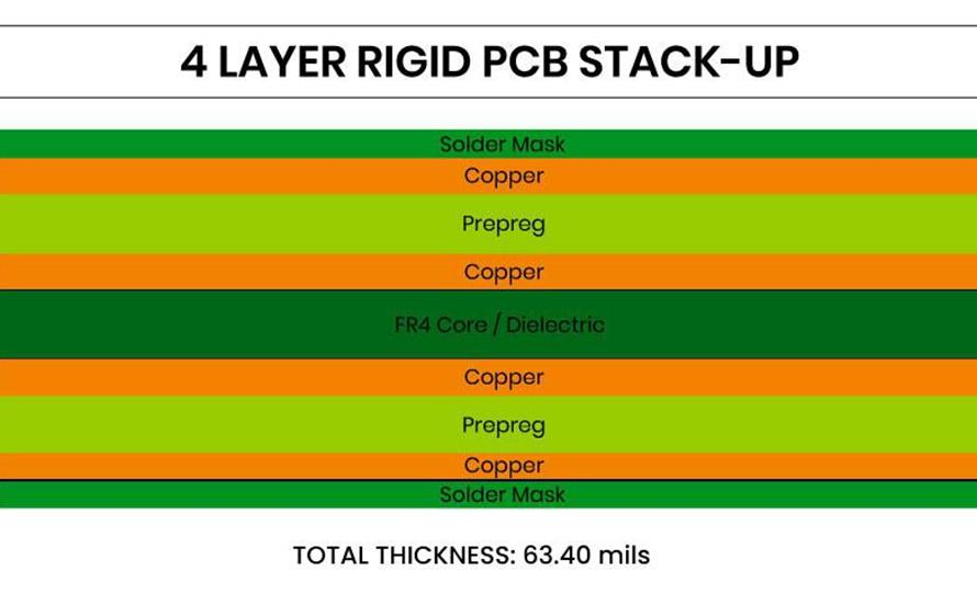
Before we delve deeper into our discussion, let’s get ourselves oriented on what is a 4 layer PCB. Four-layered PCBs are a type of multi-layer printed circuit board that offers flexible applications wherein the inner layers are used to conduct signals or powers. In comparison, the exterior areas of this PCB are used for signal routing and embedding of components.
The standard setup for a four-layered PCB follows a configuration wherein there are two signal layers for VCC and GND whereas the two innermost layers are usually a GND and power plane. The innermost layers tend to be dedicated to reducing the effect of emitted electromagnetic waves which results in a PCB that’s less vulnerable to EMI.
Stack-Up Types of 4 Layer PCBs

With the introduction out of the way, let’s move on to the types of 4 layer PCB that see frequent use. Take note that the types we’ll cover are the standard structures of this type of multilayer PCB wherein their signal layers are set depending on the application and design.
Here are some of the standard stack-up types that you’ll end up using when working with four-layered PCBs:
1. Signal, Ground, Power, and Signal
In mixed signal or digital boards, using a stack-up consisting of two signal layers sandwiching the ground and power layers sees a lot of usage. In this setup, the ground plane provides adequate shielding for the top and bottom signal layers. In the case of the power layer, its positioning enables it to deliver ample amounts of electric power to the configuration it is integrated into.
2. Signal, Power, Ground, and Signal
Swapping the power and ground signals in the stack-up can be an alternative stack-up configuration. This setup delivers the same results as the previous setup but this one is made for a different application – this stack-up is meant for electrical setups that demand extra shielding capabilities.
3. Ground, Power, Ground, and Signal
Sandwiching the power layer between two ground planes is great for a 4 layer PCB if you are working on projects that utilize RF and microwave signals. The intent in sandwiching the power layer between the ground planes is to avoid noise coupling and to preserve the PCB’s signal quality at high frequencies, thus facilitating optimal PCB performance.
Materials Used to Fabricate 4 Layer PCBs

Now that we’re familiar with some of the stack-ups or layer configurations used in a 4 layer PCB, let’s move on to the materials used. Take note that the materials we’ll cover are crucial in the successful fabrication of four-layered printed circuit boards as they enable key functions or allow components to stay in place.
With that said, listed below are the materials utilized in successfully manufacturing four-layer PCBs:
1. Copper Foils
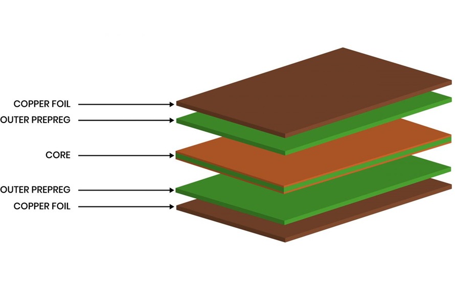
Let’s begin our discussion by covering what is a copper foil. Copper foils are best described as thin sheets or layers of copper placed on the surface of a 4 layer PCB. The intent for placing a copper foil is to set up the traces that serve as electrical pathways where currents can flow through to reach components on the PCB.
2. Solder Paste
The next material we’ll discuss is the solder paste. Solder paste is best summed up as molten metal that’s used to keep circuit board components intact when applied. Just keep in mind that after soldering, some of the solder paste will be removed if there’s still some remaining on the PCB surface – the intent for this is to facilitate surface consistency.
3. Insulating Layers
Insulating layers are a must-have on every 4 layer PCB as they function as a barrier to separate the conducting layers; aside from providing electrical insulation. These insulating layers aren’t placed into a PCB right away since they have stringent requirements such as the right dielectric constant.
4. Silkscreen Layer
Silkscreen layers are used in multi-layer PCBs to print labels, component markers, and other important identifiers on the PCB’s surface. This layer’s functions include assisting with PCB assembly during fabrication and fault detection during troubleshooting.
5. PCB Substrate
The last material needed to create a 4 layer PCB that we’ll cover is the substrate. These materials serve as the building foundation for every printed circuit board as they also offer mechanical support for all embedded or drilled components on the surface. There’s a plethora of PCB substrates that you can use; with some listed below:
- FR-4 or Fire-Resistant 4 substrates – This substrate is the most ubiquitously-seen type in printed circuit boards. The substrate boards are made out of sheets of woven glass fibers which gives it decent durability. However, its main selling point is that FR-4 substrates provide excellent insulation and very solid mechanical strength.
- FR-1/2/3 substrates – This substrate type is almost similar in every way to the FR-4 substrate; but is weaker performance-wise. FR-1, 2, or 3 substrates are best utilized in applications that demand less electrical power.
- Ceramic substrates – This substrate type tends to see usage in specialized and intense work situations due to their excellent electrical power and heat tolerance – with examples being setups that demand high-electric performance or high heat tolerance.
- Flexible substrates – This substrate type utilizes tensile or easily bent materials such as polyimide to produce multi-layered flexible printed circuit boards. PCBs that utilize flexible substrates are used in setups that require them to squeeze through a gap that can’t entertain larger PCBs.
Stack-ups and Materials make for Quality 4 Layer PCBs
To sum up what we’ve covered, a 4 layer PCB is a type of multilayer printed circuit that sees a lot of usage in different applications. It also has a lot of variations in which the signal, ground, and power layers are changed around to fit a specific application. However, to create a quality four-layered printed circuit board, you’ll need materials ranging from the substrate to copper foils to fabricate it for the desired use.

