BC557 Transistor – Pin Diagram, Specifications, Datasheet
Hello friends! Welcome back to ElectroDuino. This blog is based on the BC557 Transistor – Pin Diagram, Specifications & Working Principle. Here we will discuss the Introduction to the BC557 transistor, Pin diagram, How it Works, Specification, Features, Equivalent, Applications, and Download Datasheet.
Introduction
The BC557 is a famous three-terminal semiconductor device used to switch or amplify electrical power & electronic signals in electronic circuits. It is a bipolar junction transistor (BJT) that falls under the family of PNP transistors i.e. one N-doped layer stands between the two P-doped layers. This is a general-purpose transistor available in a tiny package like TO-92. The BC557 has an hFE rating range from 125 to 800 which makes it an ideal transistor to use as a small signal amplifier in electronic circuits. The HFE ratings are determined by the last letter after the transistor number, for example, for the BC557A transistor hFE ratings are 110-220, for the BC557B transistor it is 200-450 hFE and for the BC557C transistor it is 420-800 hFE. Another good feature of this transistor is the maximum collector dissipation is 500 milliwatts. The maximum collector current of this transistor is 100mA i.e. we can drive loads of a maximum of 100mA through the transistor.
BC557 Transistor Pin Diagram/Pin Configuration/Pinout
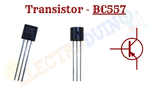
The BC557 transistor has three terminals/Pins called collector, base, and emitter, these are commonly used for external connection with the electronic circuit. The pin configuration/ Pin diagram and functionality is discussed below.

| Pin No | Pin Name | Symbol | Functionality |
| 1 | Collector | C | The Current flows in through the collector terminal |
| 2 | Base | B | The base terminal Controls the biasing of the transistor |
| 3 | Emitter | E | The flow of current drains out through the emitter terminal |
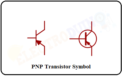
Symbol
PNP transistors have very similar schematic symbols to that of an NPN transistor. But the only difference between the NPN and PNP symbols is the direction of the arrow on the emitter. In the case of the PNP transistor, the point of the arrow is inward, whereas in the NPN transistor the point of the arrow is outward. Generally, the BC557 transistors have two types of symbols that are used in different schematic/circuit diagrams.
Working of BC557 Transistor
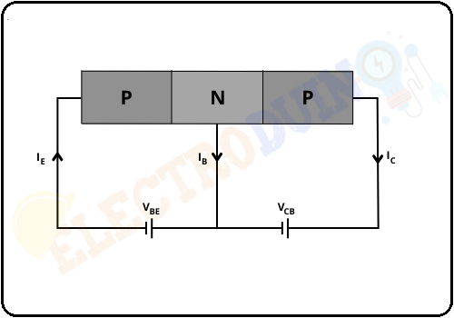
A transistor is a device consisting of 2 P-N Junction diodes connected back-to-back. In PNP transistors, one n-type semiconductor is doped with two p-type semiconductors; whereas in NPN transistors, one p-type material is placed between two n-type materials.
BC557 is a PNP BJT Transistor; in which the majority carriers are holes. It has two working states, one is Forward Bias and another one is Reverse Bias. In forward bias, BC557 works as a switch, and the same transistor works as an amplifier in reverse bias. This is a current controlled transistor in which only a small amount of current is present in the base terminal that is used to control the large current present in the other two remaining terminals.
There is a point to be noted that when our BC557 transistor is switched off the current would be present at the base terminal otherwise there will be no flow of current at that very terminal i.e., the flow of current would not be there when the transistor would be switched on.
How to use BC557 Transistors?
The BC557 family of transistors have a large use in the world of switches and amplifiers, which we can say are the two main uses of any transistor existing in the electronics arena.
BC557 Transistor as a Switch
BC557 is a PNP transistor. When this transistor is used as a switch, it is operated in Saturation and cut Off region. The transistor acts as an open switch during forwarding bias conditions and acts as a closed switch during reverse bias conditions. We can obtain this biasing by providing the necessary amount of current towards the base terminal (the maximum biasing current which is allowed is 5 mA). If we will take the current value more than the max. biasing current then it may damage our transistor.
Now going to the connection part; the transistor must be connected to the base terminal in series. The emitter-base voltage (VBE) must be 5 V. The base current (IBC) mainly depends upon the collector current (ICC). The base resistance can be calculated from the formulae mentioned below,
RB = VBE/IBC
When we grounded the base pin of this transistor, then it starts working as Forward Bias. In this condition, this transistor allows the flow of current through the collector & emitter. So, the transistor act as a closed switch.
when we will provide positive voltage at the base pin of this transistor, then it starts working as Forward Bias. In this condition, this transistor doesn’t allow the flow of current through the collector & emitter. So, the transistor act as an open switch.

BC557 Transistor as An Amplifier
As previously mentioned, the BC557 transistor functions like an amplifier when it is reverse biased. This transistor may use different configurations namely, Common collector, Common base, and Common emitter to amplify current, voltage, or power. But, among all the configurations mentioned above the most generalized one is the common emitter configuration. While using the said transistor as an amplifier there is a DC current gain which can be measured with the help of the given formulae,
IDCG = ICC/IBC
Where, IDGC = DC Current Gain
The two terminals namely the emitter and collector will be made forward biased by connecting the base pin to the ground. The given transistor gets reverse biased when a signal is provided to the base terminal. The maximum current that can be supplied throughout the collector terminal is100 mA. The voltage allowed across CE is 200 mV and that across BE is 900 mV.
Specification of BC557 Transistor
- Package type: T092
- Transistor type: PNP
- ICC max value: 100 mA
- Employing and repository temperature range: -65 to +150 oC
- VCE value = -45 V
- VCB value = -50 V
- VBE value = -5 V
- IDGC range = 125 – 800
- Transition frequency = 100 MHz
- Collector Dissipation = 500 mW
- Peak collector current = 200 mA
- Junction temperature = 150 oC
Features
BC57 Transistor consists of many amazing features which we will come across in the next few points,
- The transistor is having advanced process technology along with less error voltage
- Its switching speed is really appreciable.
- Its current and power handling capability is high enough of proper functioning.
- Its complete voltage operation is also a perk.
Equivalent Transistor
Alternative transistors for BC557 are BC558, BD140, TIP42, BC157, TIP127, 2N3906 and 2SA1943
Application
BC557 Transistor being a PNP BJT has numerous uses in electronic circuits and it is mentioned to be very useful to circuit designers. Some of its uses are listed below,
- Used in amplifier modules and driver modules.
- Used within electronic bells, radios, etc. as an audio amplifier.
- It has a wide range of uses in robotics and instrumentation projects.
- Also used to control the flow of current in motors.
- Switching purposes has one of its main uses.
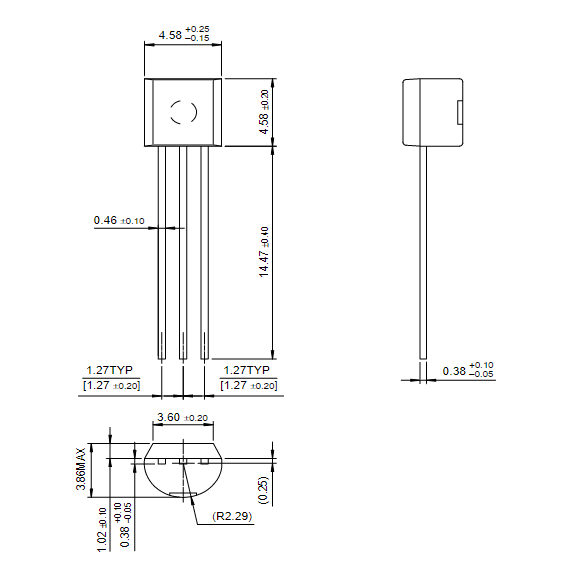
2D-Model and Dimensions
